Process Control of Ultra Thin Films at Micro Spots
As electronic devices and products become smaller, so do the semiconductors and components required to make them. This miniaturization requires ultra thin film capabilities along with reliable measurement methods in order to ensure expected performance and quality while still maintaining cost efficiencies.
In addition to the overall need generated by the increase of smaller components, additional benefits of ultra thin films include (but aren't limited to) providing flat services, higher through-put efficiencies, and ideal soldering surfaces. Common methods to achieve these ultra thin films include electro-plating, immersion coating, and vapor deposition methods - both physical (PVD) and chemical (CVD).
In addition to the overall need generated by the increase of smaller components, additional benefits of ultra thin films include (but aren't limited to) providing flat services, higher through-put efficiencies, and ideal soldering surfaces. Common methods to achieve these ultra thin films include electro-plating, immersion coating, and vapor deposition methods - both physical (PVD) and chemical (CVD).
WHY X-RAY FLUORESCENCE?
While other technologies are available to measure thin films, ED-XRF technology offers a non-destructive method that is relatively simple to operate, does not require consumables, and allows for high through-put. These advantages make x-ray fluorescence a critical tool in process control laboratories...positively impacting different industries and a variety of applications.
However, appropriate process control in these situations require a different category of x-ray fluorescence (XRF) analyzer from those used in basic coating thickness applications. The different XRF systems are required for two primary reasons - the obvious is to achieve thinner thickness measurements and the other is the need to measure smaller spots on the smaller components.
The first of these requirements, ultra thin measurement capability, is achieved with overall component configuration but the use of a high performing detector technology is a critical aspect. The Hitachi FT-160 XRF Analyzer features the highest resolution detector to achieve high energy resolution and count rates...both are critical in achieving optimum performance on ultra thin films. In addition to improving accuracies, the detector selected by Hitachi High-Tech offers the added benefit of faster measurement times when compared to competitive ED-XRF analyzers.

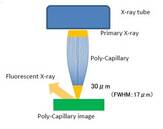
The second aspect of ultra thin measurement requirements, micro-spot capabilities (those under 100um), requires advanced x-ray optics. For this reason, the Hitachi FT-160 is designed with poly-capillary optics - an optical element that works like a convex lens to focus x-rays onto a micro-spot by using several thousand glass capillary tubes. The FT-160 provides a FWHM spot size of 17um, which is a proven size to measure in the small, localized, areas.
COMMON APPLICATIONS:
Ultra thin films are seen in semiconductor fabrication, printed circuit board manufacturing, and in thin film solar cells with applications ranging from a variety of films on silicon substrates (SiO2, AlSi, Ti, TiN, Pt, Al, and BPSG) to Au/ENi/Cu (aka ENIG) and Au/Pd/ENi/Cu (ENEPIG) or CIGS and CdTe for solar cells.
Additional Reading: Measuring ENIG and ENEPIG
Application Specialists at Eastern Applied Research and Hitachi High-Tech Science Corporation are developing application briefs on the most common ultra-thin film applications but please contact us if you would like to submit samples to review the Hitachi FT160 performance on a specific testing goal you have.
The team at Eastern Applied Research welcomes a discussion on your organizations thin film requirements and how ED-XRF capabilities can enhance your process control efficiencies.
